Recently, when I drew the PCB, I felt that I was not familiar with a lot of electronics, so I searched Wikipedia to organize the basics.
🌟History of Electronics
Vacuum Tube Period
Vacuum tube can be divided into diode, triode, tetrode, pentode and compound tube, etc.
In 1904, John Ambrose Fleming invented the diode, and in 1906, Lee De Forest invented the triode.
Electronics at this time was mainly “radio technology”.
Transistor and Integrated Circuit Period
In 1948, John Bardeen, Walter Houser Brattain and William Shockley of Bell Labs invented the transistor.
In 1958, Jack Killby invented the Integrated Circuit (IC).
⭐️Diode

Early vacuum diodes, later semiconductor diodes were developed.
Structure
A crystalline sheet of semiconductor properties is connected to two terminals by a PN junction.
PN Junction
A piece of semiconductor crystal (e.g. silicon crystal) is doped with a small amount of phosphorus on one side so that the free electron concentration is higher and negatively charged, an N-type semiconductor, and a small amount of boron on the other side so that the hole concentration is higher and positively charged, a P-type semiconductor. The contact surface in the middle forms a transition layer and becomes a PN junction.
Characteristic
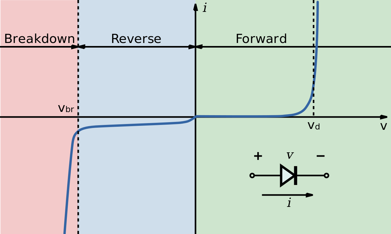
Diodes only allow current conduction in one direction, i.e. current flow in the forward direction and blocking in the reverse direction.
The current-voltage characteristic curve of a diode is nonlinear.
⭐️Triode
The vacuum triode has an amplifying function and was the first electronic amplifier. It was replaced by the transistor from the 1970s onwards.
⭐️Transistor
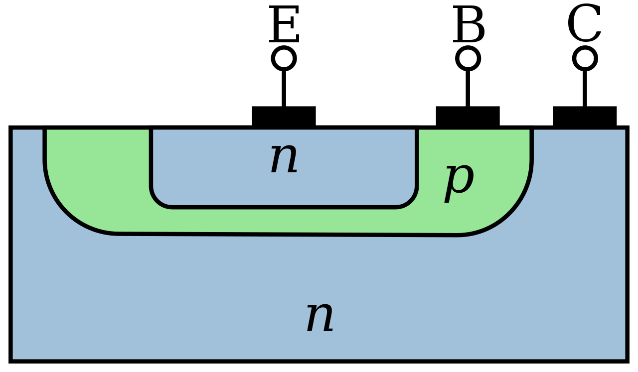
Structure
A transistor is made of three parts of semiconductor with different degrees of doping. The boundary between two different dopants forms a PN junction, so there are NPN type and PNP type. It has three external endpoints (called poles).
Characteristic
When a transistor operates in the linear region, it becomes an “amplifier”. It is commonly used in analog circuits.
When the transistor is either completely off or completely on, it is called a “switch”. Commonly used in digital circuits.
Classification
There are two main types of transistors: Bipolar Junction Transistor (BJT) (commonly known as a triode) and Field Effect Transistor (FET) (also known as a unipolar transistor).
When a BJT operates, both electron and hole carriers are flowing; when a FET operates, only a single type of carrier is flowing.
BJT
The BJT has three poles Emitter, Base, and Collector.
A small current from the emitter to the base causes the impedance between the emitter and the collector to change, thus changing the current flowing through it. That is, the base-emitter current controls the collector-emitter current (which can also be thought of as voltage control).
In the amplification zone, it can be approximated that the former is a constant value and the latter is a number of times the former, and the transistor acts as a current amplifier.
NPN Type
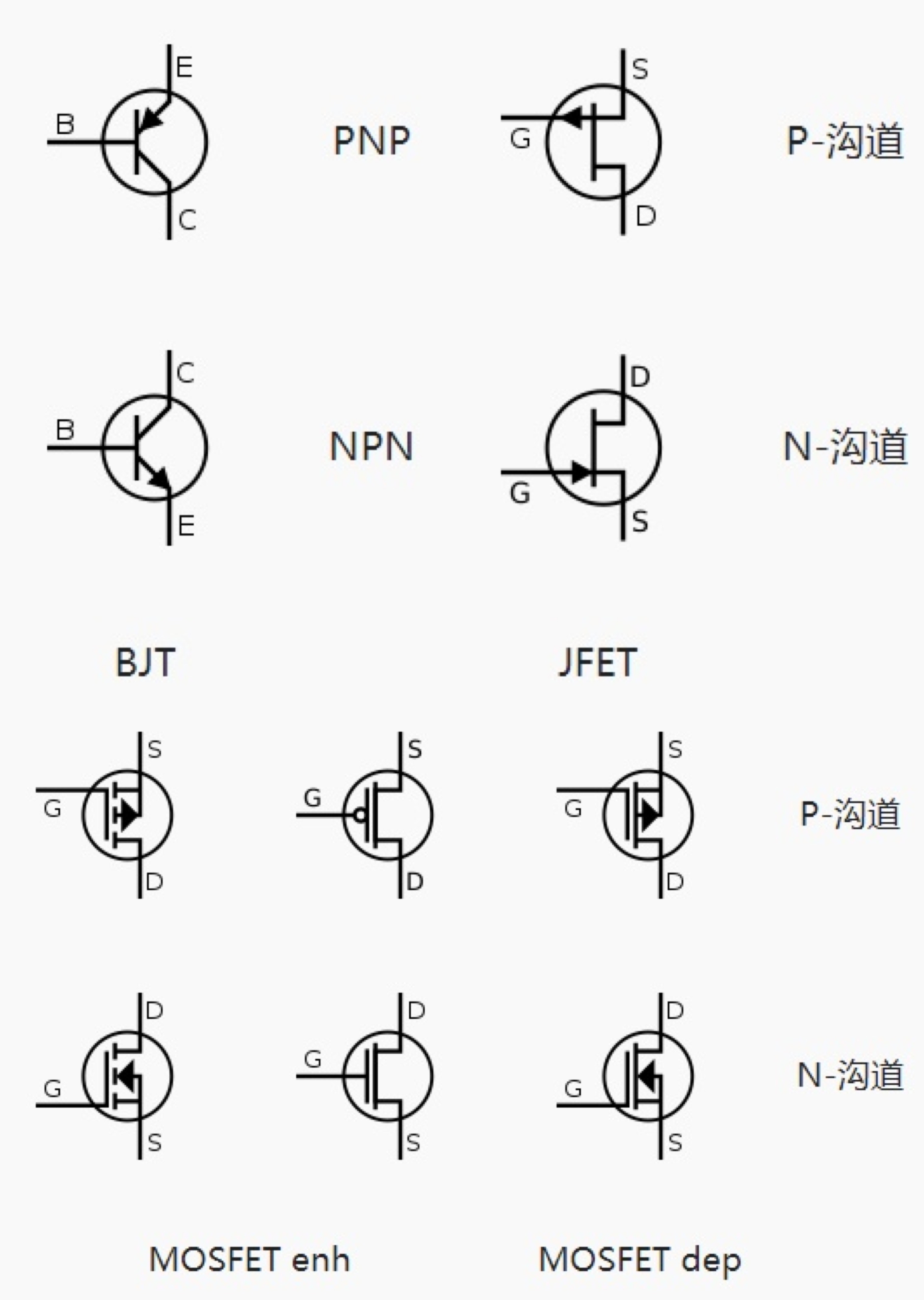
The arrow (indicating the emitter current direction) points outward, i.e. from the base to the emitter.
Most of the BJTs used today are NPN types.
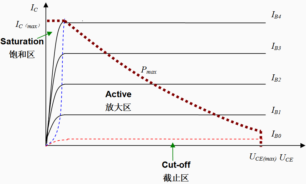
Define the working area according to the bias of the emitter junction (base-emitter) and collector junction (base-collector):
- Forward amplification zone/amplification zone (collector-emitter current is approximately linear with base-emitter current): forward bias of the emitter junction, reverse bias of the collector junction.
- Reverse amplification region (hardly used): emitter reverse bias, collector junction forward bias;
- Saturation region (can be represented as high level in digital logic): both PN junctions forward biased;
- Cut-off zone (can be represented as low in digital logic): both PN junctions reverse biased;
- Sudden collapse: the reverse bias current of the collector junction is too high and the PN junction is broken down.
PNP Type
The arrow points inward, i.e., from the emitter to the base.
The voltage description of the working area of the PNP type is opposite to that of the NPN type.
Three Types of Amplifier Structure
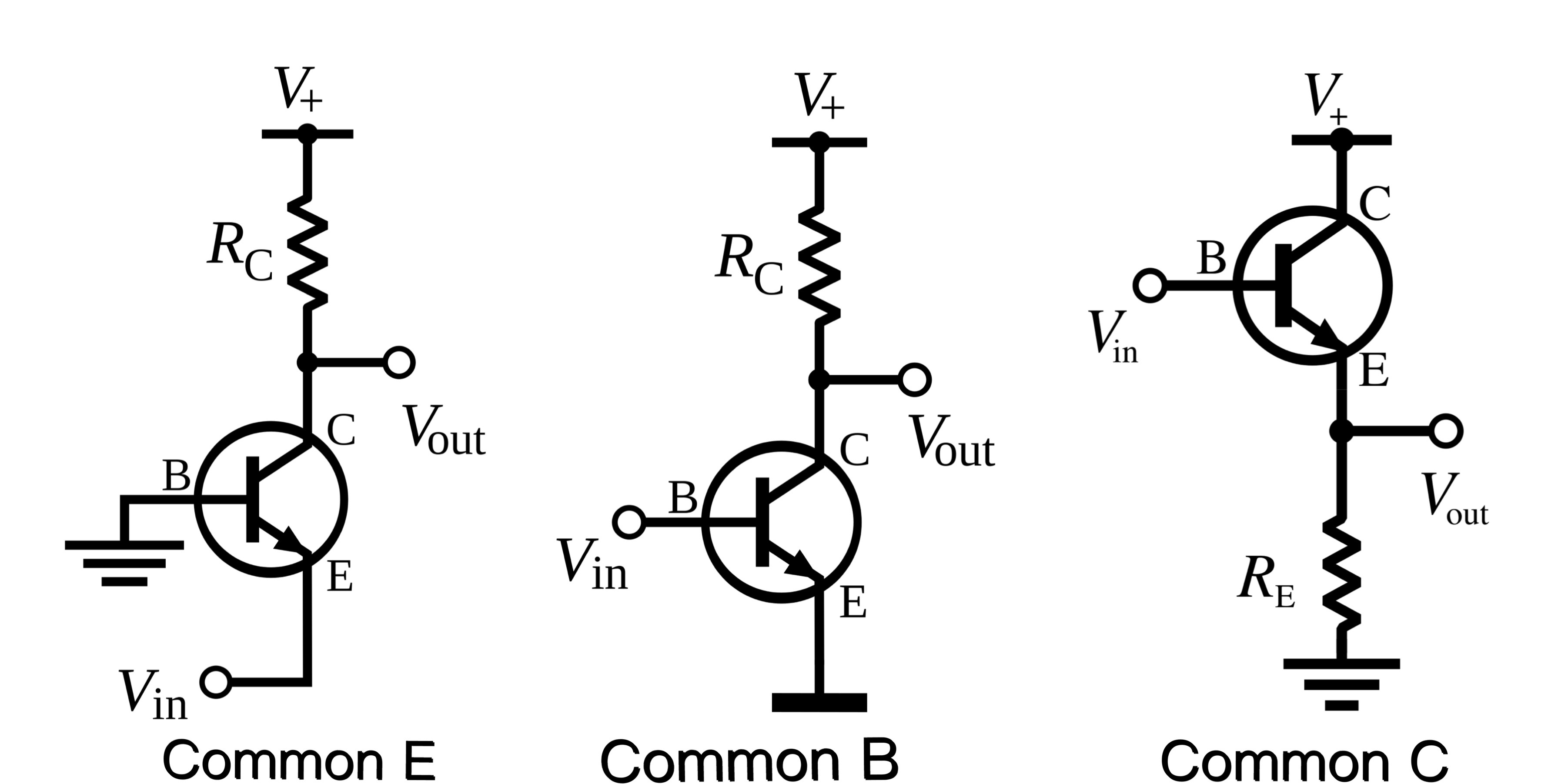
Common Emitter
The base is used as the input, the collector as the output, and the emitter is common (i.e. grounded, or connected to power). Similar to the common source of FETs.
Usually used in power amplifiers, RF circuits, and low-noise amplifiers.
Common Base
That is, the base is grounded (or connected to a power supply). Similar to common gate of FET.
Usually used in current buffers, voltage amplifiers. Not commonly used in low frequency circuits, commonly used in high frequency circuits.
Common Collector
That is, the collector is grounded (or connected to the power supply). Similar to common drain of FET.
Usually used in voltage buffers, negative feedback amplifiers.
FET
Practical devices are the Junction Gate Field-Effect Transistor (JFET) and the Metal-Oxide-Semiconductor FET (MOSFET). Both are based on the same principle, but the former uses a PN junction and the latter uses a Schottky junction (a junction between a metal and a semiconductor).
The three poles of a FET are Gate, Drain, and Source (corresponding to B, C, and E of a BJT). All FETs except JFETs have a fourth pole, called body, base, bulk or substrate. This fourth pole modulates the FET to operate.
JFET
There are two types of JFETs: N-channel and P-channel.
Structure and Principle
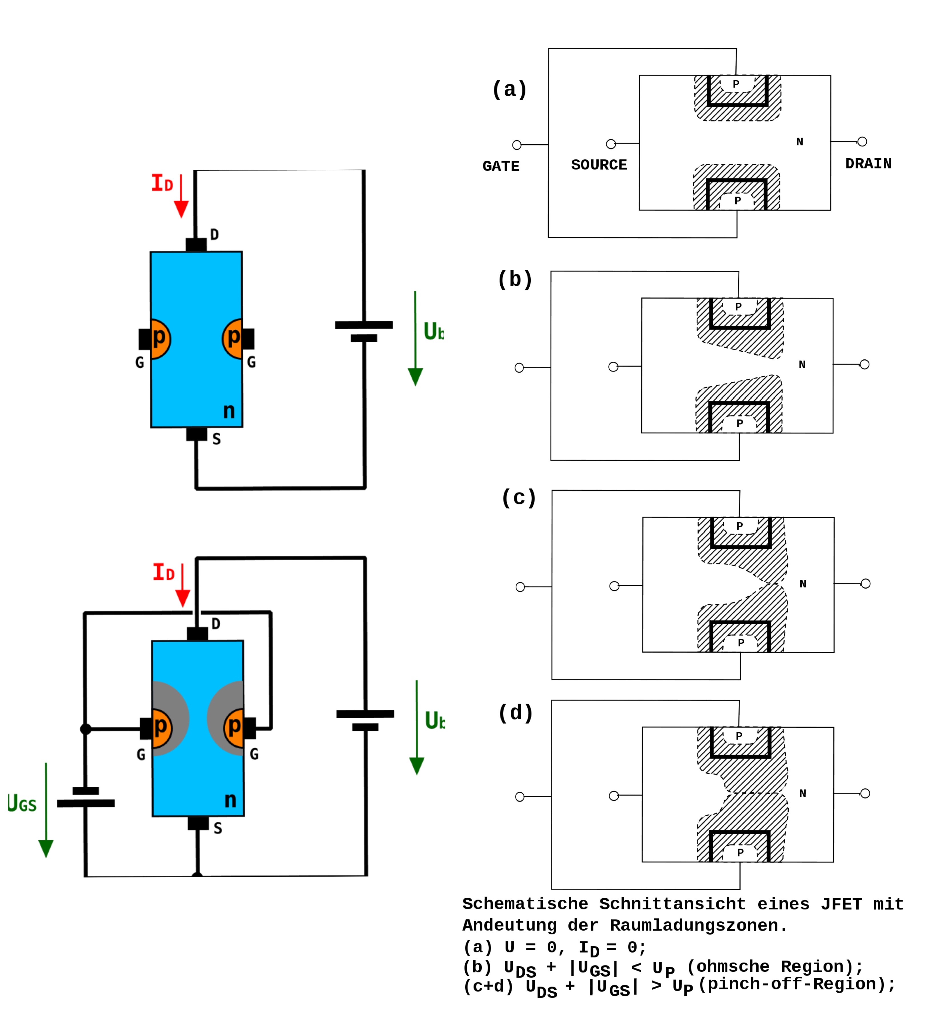
An N-channel JFET is an N-type semiconductor surrounded by a P-type semiconductor.The N-channel between Source and Drain forms a PN junction with the P-zone of Gate.Gate acts as a control.
Up is the pinch-off voltage. After clip-off, it is equivalent to a constant current source (I_DSS).
Symbol
The arrow indicates the polarity (from P to N) of the PN junction formed by the channel and gate, and also the direction of current under forward bias.
MOSFET
MOSFETs are classified as NMOSFETs and PMOSFETs, and can be classified as enhanced or depleted.
MOSFETs conceptually belong to Insulated-Gate Field Effect Transistor (IGFET). IGFETs mostly refer to MOSFETs.
Structure and Principle
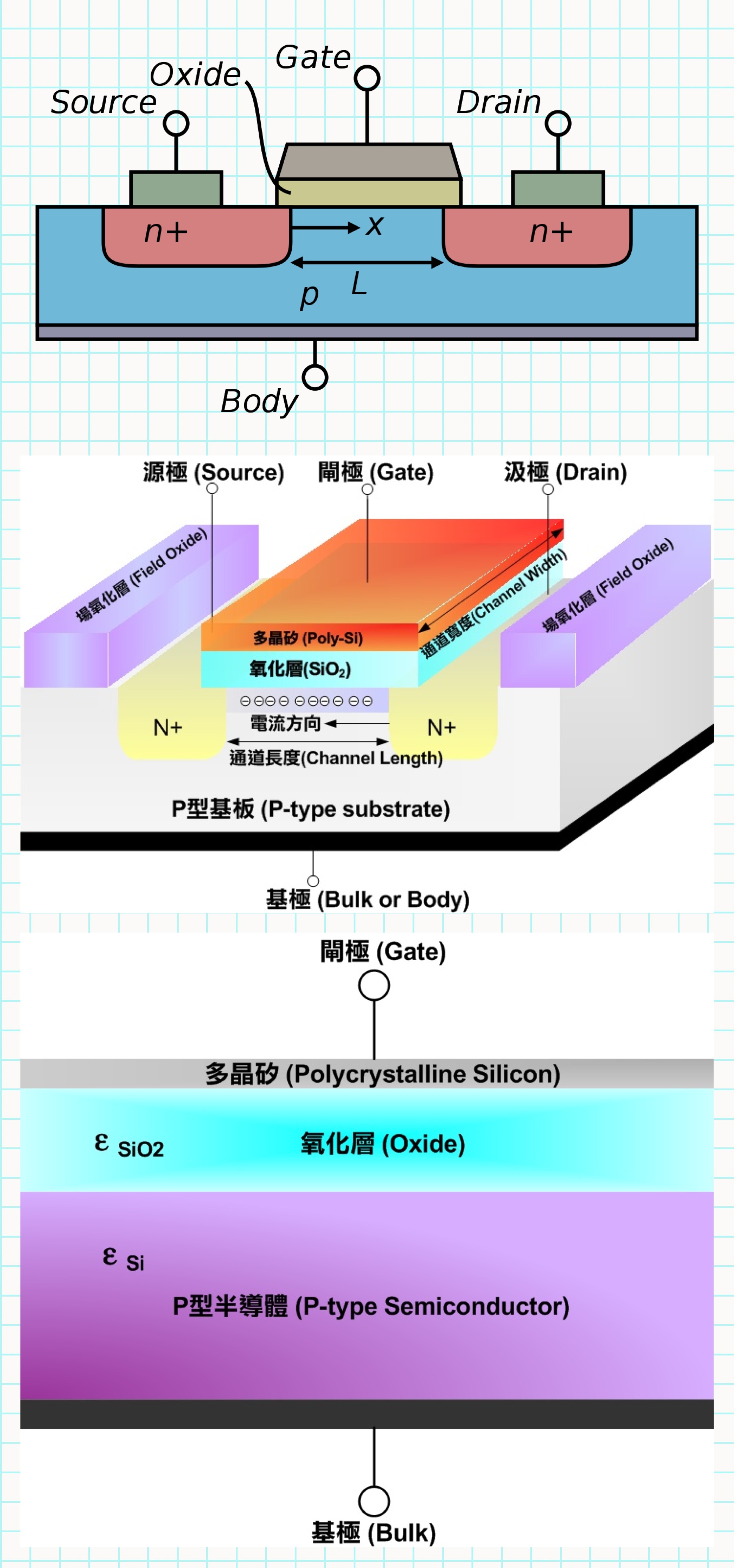
MOSFETs have Body in addition to Source, Drain and Gate.
The core of the MOSFET is the MOS capacitor in the center, with the Source and Drain on the left and right sides.
The structure of the MOS capacitor is “Metal (often replaced by polysilicon) - Oxide (SiO2) - Semiconductor”, where the oxide is equivalent to the dielectric in a capacitor.
Working Area
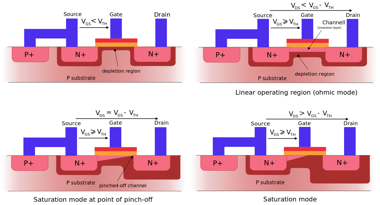
There are three working modes, depending on the bias voltage applied at the three poles of the MOSFET. Taking the enhanced NMOS as an example:
When |VGS| < |Vth|, it is in the cut-off region and does not conduct. |VGS| is the bias difference from Gate to Source and |Vth| is the critical voltage of the material;
When VGS > Vth and VGD > Vth, it is in the linear region, equivalent to a voltage controlled resistor, with a linear current-voltage relationship;
When VGS > Vth and VGD < Vth, it is in the saturation region.
Symbol
Changing the dashed line to a solid line is a depletion type MOSFET.
⭐️Logic Circuit
The BJT logic circuits are TTL (Transistor-Transistor Logic) and ECL (Emitter Coupled Logic), and the MOSFET logic circuits are CMOS (Complementary Metal- Oxide - Semiconductor).
TTL
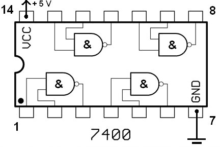
TTL is a digital integrated circuit consisting of transistors, diodes and resistors. The most common is the 74 series.
TTL is fast, CMOS is slow, but power saving and lower cost than TTL. TTL is now used mainly for educational or simpler digital circuits.
CMOS
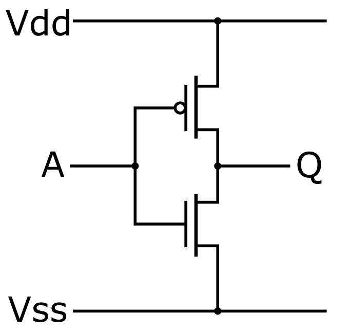
CMOS consists of a pair of NMOS and PMOS.
CMOS only consumes energy when switching between start-up and shutdown.
ECL
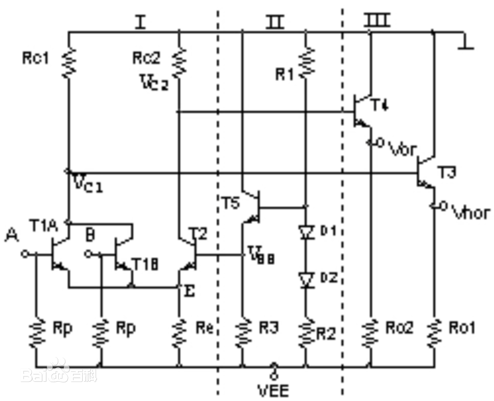
ECL is fast. The swing is small and the anti-interference capability is weak.
The first part of the diagram is a switch to realize the “or/ or not” function; the second part is a reference voltage source to realize the temperature compensation function; the third part is an emitter follower to realize the output and isolation function.
Comments