This is one of my course papers, which details the design of the Front-End Electronics for the Main Drift Chamber of the Super Tau-Charm Facility.
(The following has been modified and formatted in an informal paper format to make it easier to read. )
Abstract
The Super Tau-Charm Facility (STCF) is a new-generation positron collider planned to be built in China, which is a continuation of the currently operating Beijing Electron Positron Collider II (BEPC II) and its companion Beijing Spectrometer III (BES III), which are dedicated to the physics of the τ-charm region.
The Main Drift Chamber (MDC) is one of the main sub-detectors of the STCF detector, which is mainly used for final-state charged particle trajectory, momentum measurement and particle identification. The weak analog electrical signals output from the detector need to be configured with a set of Readout Electronics system to process them, amplify them and convert them into digital signals to form case data that can reflect the characteristics of the particles for the Data Acquisition System (DAQ) to rebuild and record the physical cases, which are provided to physicists for offline analysis.
This paper describes the overall structure of the STCF MDC front-end readout electronics system prototype circuit verification board, as well as the preliminary design of the analog daughter board. The MDC readout electronics consists of the Front End Electronics (FEE) module and the Readout Unit (RU) module, corresponding to the analog daughter board and the digital mother board, respectively. The whole system is a 16-channel system with 2 channels on a single daughter board, and every 2 daughter boards are connected to 1 mother board. The daughter board contains 4 parts: TIA and ADC drivers circuit, calibration circuit, power supply circuit and main control circuit.
For now, PCB layout, soldering and preliminary testing have been completed, and the joint test of electronics and detector is underway to prepare for further electronics system design.
Background and Significance
Particle physics studies the composition and interaction of matter at a deeper level than the atomic nucleus, which is closely related to the origin and evolution of the universe, leading the development of mankind’s basic view of space and time, and is the science at the forefront of mankind’s understanding of the world. At the same time, it has given rise to many new cross-disciplines, spawned the construction of specialized large-scale scientific devices (e.g. colliders and accelerators), and developed into a large-scale comprehensive platform for multidisciplinary cross-frontier research.
Accelerator-based particle physics experiments are one of the most effective means of studying the microscopic material world. Today’s accelerator-based particle physics experimental research can be categorized into high-energy frontier and high-brightness frontier, two different frontiers that complement each other. As one of the important representatives of high-brightness frontier accelerator experiments, the Positron-Negative Electron Collider – tau-charm facility operates in the tau-charm energy region (center of mass energy of 2-5 GeV) and has been one of the key focuses of attention in the field of particle physics research in the past 40 years. The Beijing Positron-Negative Electron Collider/Beijing Spectrometer (BEPCII/BESIII) experiments built under the auspices of China have historically made world-renowned physics achievements such as tau lepton mass measurements, R-value measurements, and the discovery of X (1835), laying the foundation of China’s high-energy physics research.
However, due to the constraints of geographic location and some infrastructural conditions, BEPCII/BESIII does not have the space and potential to further improve its performance significantly. In addition, with the aging of the detectors and the competition from other particle physics experiments (e.g., BELLE-II, LHCb, etc.), BEPCII/BESIII will complete its historical mission in 5-10 years. In view of the importance and needs of physics in the tau-charm energy region mentioned above, as well as the current status of experimental research in this energy region both at home and abroad, China has proposed to build a new generation ultra-high-brightness positron-negative electron collider – Super Tau Charm Facility – to continue to maintain its leading position in this research field.

The overall layout of the STCF is shown above. It includes an accelerator facility with a brightness greater than 0.5 × 1035 cm-2s-1, a center-of-mass energy of collisions covering 2-7 GeV, a multifunctional magnetic spectrometer capable of adapting to high-brightness environments to meet the needs of physics research, and related infrastructure.
The core technology of the STCF accelerator is how to break through the peak collisional brightness. In order to realize the ultra-high brightness, STCF will adopt the widely used flat symmetric positive and negative electron beams and double-ring structure. The STCF detector is a large-scale integrated detector consisting of a combination of multiple particle detectors for the detection and species identification of end-state particles (protons, π, K, electrons, muons, photons, etc.) produced by collisions of positive and negative electrons.
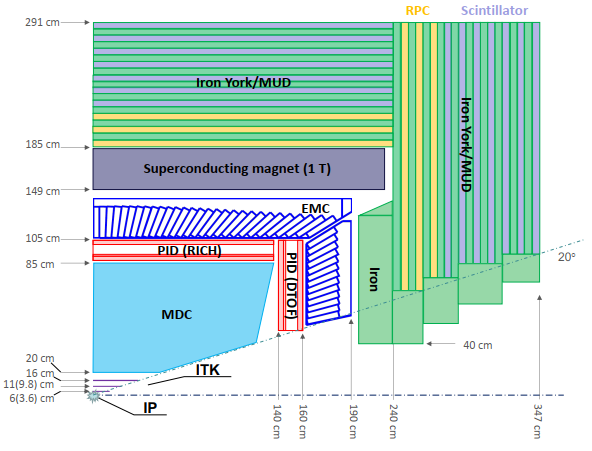
As shown in the figure above, the STCF detector consists of the Inner Tracker (ITK), the Outer Track Detector (i.e. MDC), the Particle Identification (PID), the Electromagnetic Calorimeter (EMC), the Superconducting Magnet, and the Muon Detector (MUD).
Among them, the Outer Track Detector is a large cylindrical precision drift chamber surrounding the ITK,which carries out the main functions of charged particle trajectory and momentum measurements, and is therefore also called the Main Drift Chamber (MDC). The MDC also measures the loss of ionization energy of charged particles, and is used to identify low-momentum charged particles. The MDC is filled with gas, and has a large number of fine wires arranged axially, forming a large number of drift cells. By measuring the drift time of the ionized electrons generated by the charged particles in the cells, the corresponding drift distance can be obtained, which together with the position of the anode filaments can be used to obtain the position of the charged particle trajectory. The STCF MDC has a total of 48 filament layers, and the positional resolution of the individual filaments is 120 µm.
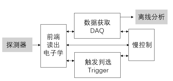
As shown in the figure above, the basic composition of the electronics system in particle physics experiments is the front-end readout electronics, the trigger system, the data acquisition system and the slow control system (you can see Basic Components of Electronics of Particle Physics Experiments). In order to acquire and process the output signals of the STCF MDC, it is necessary to design the electronics system that accompanies it.
The function of the Front-End Readout Electronics is to amplify the weak electrical signals from the detector outputs, digitize them, and convert them into data reflecting the properties of the particles for reconstruction of the physical instances and recordings by the data acquisition system. The front-end readout electronics can provide the trigger system with information on which parts of the detector have been struck by particles and the energy deposition of the particles in the detector after the initial processing of the detector output signals, as the original conditions for triggering. Front-end readout electronics also need to carry out the necessary pre-processing of the data, such as data compression, data normalization and so on.
The function of the trigger system is to analyze the data provided by the front-end electronics in real time, and to select physically interested instances from a large amount of instance data, while discarding the false instance data.
The function of the Data Acquisition System is to collect and assemble the data digitized by the readout electronics system into a complete instance data recorded in mass memory.
Overall System Structure
MDC Readout Electronics
In the preliminary conceptual design of the STCF MDC, the MDC contains 11,520 cells and the total number of readout electronics channels for the signals is also 11,520. The readout electronics are set up in endcaps, which are made of 15 mm thick aluminum plates for mechanical support. The results of the beam simulations show that the first (innermost) layer of the MDC is subjected to the highest background count rate (approximately 200 to 400 kHz), which can severely interfere with the measurement of the charged trajectories of the signal events. The results of the GARFIELD simulations show that, due to the uncertain distribution of the electrons by the distance from the particle trajectories to the wires, the signals in each cell last from 200 to 500 ns. Therefore, the MDC readout electronics system requires highly accurate time measurements (~0.5 ns RMS) and charge measurements (up to 1.8 pC amplitude of the input signal).
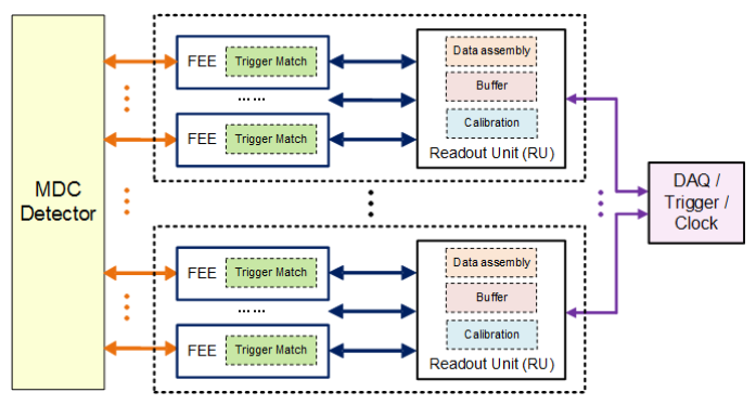
The STCF MDC readout electronics system architecture is shown in the figure above, consisting of the FEE modules and the RU modules. The readout electronics of the MDC needs to be synchronized with the system clock signal, which is received by the RU and then fanned out to the FEE. The output of the FEE is collected by the RU, which further aggregates this data and transmits the signals to the DAQ via fiber optics. The RU also receives the global trigger signal and it fans out to the FEE for trigger matching to read out valid data.
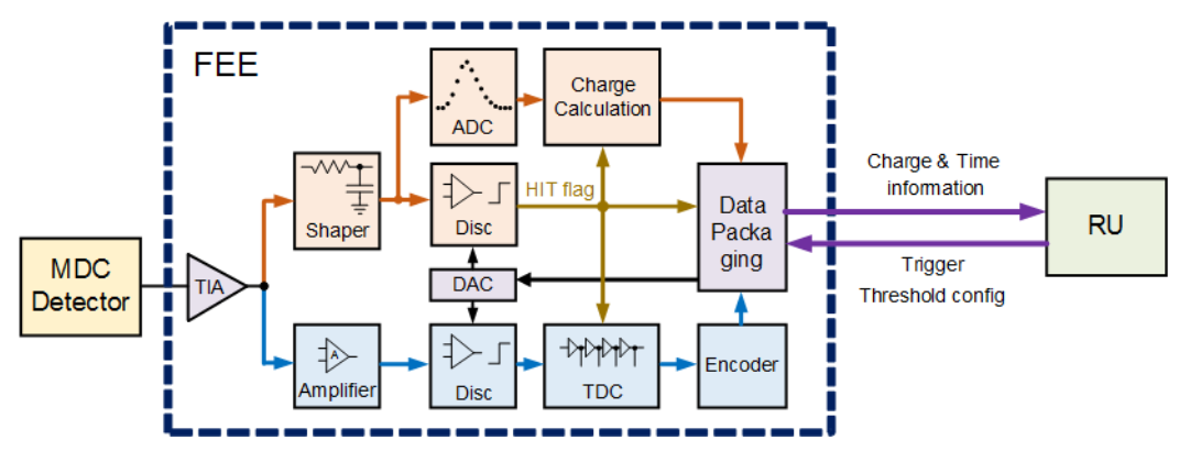
The circuit structure of the FEE is shown above. The FEE is responsible for the processing of analog signals, A/D conversion, and the measurement of time and charge information. The signal from the detector MDC is first amplified by the Trans-Impedance Amplifier (TIA) to ensure fast response for time measurement and to provide charge measurement. The output signal of the TIA is then split into two: one is connected to the charge measurement circuit and the other is connected to the time measurement circuit.
For time measurement, the threshold of the Discriminator (Disc) is set to a low level considering the characteristic shape of the signal. In order to achieve high time accuracy, an Amplifier located before the Discriminator is used to increase the slew rate of the signal. In order to filter out noise crossing the low threshold, another high threshold discriminator is used after shaping. Then, a Time-to-Digital Converter (TDC) is used to digitize the leading edge time of the low threshold discriminator.
The charge measurement circuit uses a Shaper to improve the signal-to-noise ratio, and its output waveform is digitized by an Analog-to-Digital Converter (ADC) and sent to an FPGA for charge calculation. The output signal of the shaping circuit is fed into a discriminator with a high threshold. The output of this discriminator is used as a HIT flag to start the charge calculation process and as a “valid” condition for the time measurement of the low threshold discriminator output. In order to suppress the effects of Data Packaging, baseline recovery and digital processing on the digitized signal waveform are applied to the circuit design.
Daughter-Mother Structure for Validation Boards
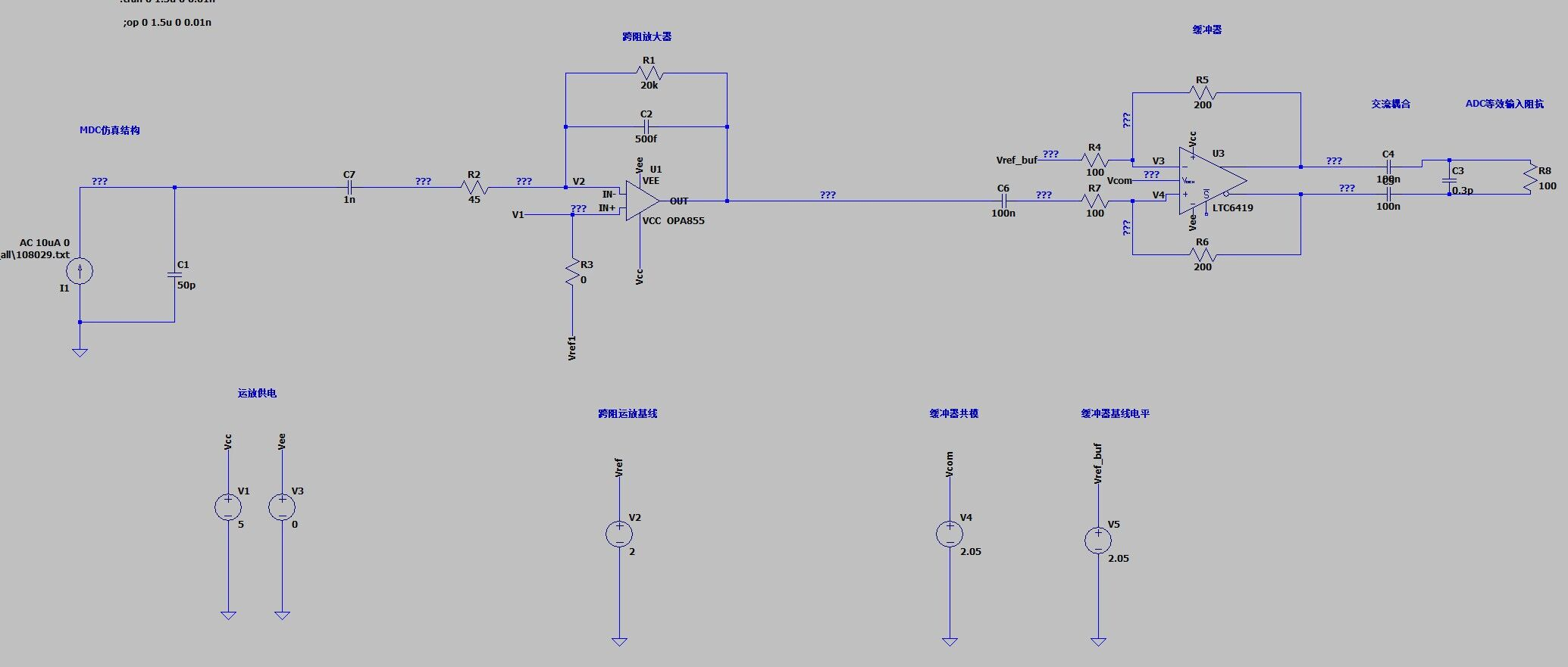
The above figure shows the circuit model and simulation performed in LTspice software. In order to further ensure the principle correctness and application feasibility of the scheme, as well as to obtain a preliminary practical test result, a verification board needs to be designed.
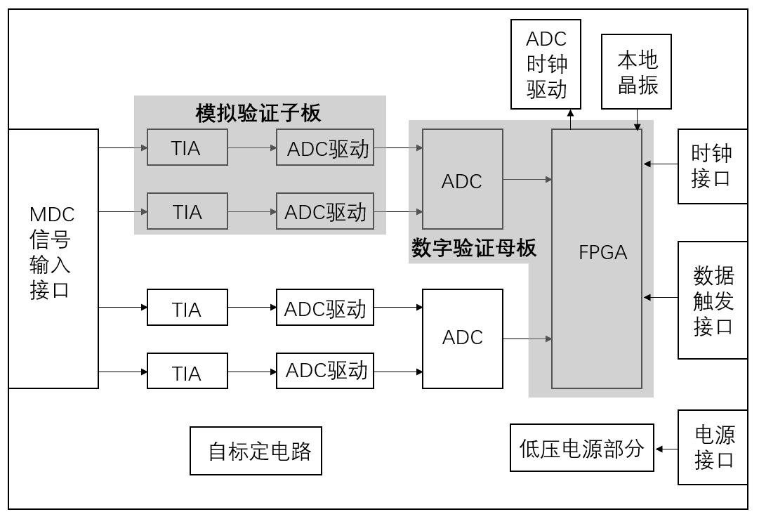
In terms of hardware structure, the verification board is designed as a flexible daughter-mother board as shown in the figure above, i.e., a combination of an analog daughter board and a digital mother board. The analog daughter board receives and conditions the analog signals from the MDC and inputs the signals to the digital mother board via differential LEMO connectors. The Digital mother board performs analog-to-digital conversion of the signals, and processes and calculates the digital signals in the FPGA, and finally outputs the desired data results to the PC through the connector. It is more difficult to use high-speed ADC to realize 32-channel signal readout, so the number of channels of a single verification board system is set at 16. 2 channels are available on a single daughter board, and a single mother board can be connected to 2 daughter boards, so a single verification board system contains 8 daughter boards and 4 mother boards.
The daughter boards mainly contain the TIA as well as the ADC driver. Since the sampling rate of ADC is between 500MHz and 1GHz, a dual-channel, 14-bit ADC chip with a sampling rate of 1GHz, GM4680-1000 is considered. In the mother board, the FPGA chip selection needs to give priority to meet the data reception requirements of the ADC to ensure the normal operation of the high-speed transceiver interface.
The system clock is provided by the local crystal or clock interface. The FPGA generates the clocks for the ADC drivers and sends them to the ADCs through the clock driver to ensure that all the ADCs work synchronously. The clock synchronization of the MDC electronics needs to be done through the clock interface.
The MDC signal input interface is determined by the output of the detector. The data trigger interface is determined by the DAQ together with the trigger system.
The calibration circuit is used for subsequent testing or self-testing of the electronics function.
Design of the Analog Daughter Board
We use Cadence to design the electronics system. First design the circuit schematic in OrCAD Capture CIS and then design the printed circuit board (PCB) in Allegro PCB Editor.
Schematic design
The schematic of the daughter board consists of 4 pages, in order of the circuits of the TIA and ADC Driver, Power Supply, Master Control and Calibration sections.
TIA and ADC Driver Section
The analog signal from the detector is fed into the daughter board through the LEMO connector, and then passes through the isolation capacitors and matching resistors into the preamplifier. A preamplifier is a circuit or electronic device placed between a signal source and an amplifier, and is designed to accept weak signals from the signal source. A preamplifier that processes charge (current) information is called a charge-sensitive amplifier.
The preamplifier uses the OPA855 chip. It is a wide-band low-noise operational amplifier with bipolar inputs for wideband transimpedance and voltage amplification. If this op-amp is configured as a TIA, its 8 GHz Gain-BandWidth Product (GBWP) is capable of achieving high closed-loop bandwidths with transimpedance gains of up to several tens of kilo-ohms. Simulation test results show that the OPA855’s -3dB bandwidth is 80MHz when the OPA855’s gain is 20kΩ and the detector’s equivalent capacitance to ground is 50pF. The OPA855’s reverse end is connected to a feedback resistor, and the forward end is connected to ground through a 0Ω resistor or can also be baselined through a Digital-Analog Converter (DAC). According to the impedance value of the MDC signal, adjust the matching resistors appropriately, and when the impedance is matched, the noise of the circuit is minimized. Bypass capacitors are placed near the power supply side to filter out high frequency noise and reduce coupling interference.
After the signal is conditioned and amplified by OPA855, it is fed into CR-RC passive filter network to facilitate the subsequent debugging. The signals processed by the filter network are sequentially isolated by capacitors and matched by resistors, and then fed into the ADC driver, which is generally placed close to the ADC. Bypass capacitors are also required near the power supply.
The ADC driver uses the LTC6419 chip. It is a dual-channel, very high-speed and low-distortion differential amplifier that converts the input single-ended signal to a differential signal to drive the ADC connected behind it, and isolates the preamplifier from the ADC and acts as a buffer. The differential ADC driver is an indispensable signal conditioning component in the data acquisition system. In this design, the differential amplification gain of the LTC6419 is configured as 2.
Power Supply Section
The external power supply enters the board through the power socket, and after a series of capacitive filtering and inductive isolation, it is fed into the Low-Dropout Regulator (LDO) component. The LDO is configured to obtain the required supply voltage for the entire board. A LDO is a type of linear DC regulator used to provide a stable DC voltage supply. It is able to operate with a smaller output-input voltage difference than a typical linear DC regulator. The LDO in this design is LT1764, which has the advantages of fast transient response and very low output voltage noise.
Main Control Section
The function of the main control section is globally control and connects the various modules between the daughter and mother boards. It mainly contains a connector that serves as the interface to the daughter and mother boards, a LEMO connector for the output signals, and several selection resistors for subsequent debugging and testing. The daughter-mother interface of this design uses Samtec’s TFM-115-01-L-D-DS model connector, which has a total of 30 pins available. It has less than 1% crosstalk between adjacent pins for signals with a rising edge of 1 ns; single-ended impedance of 48.2-50.8 Ω and differential impedance of 92.2-102.8 Ω; a bandwidth of up to 8 GHz; and can pass current signals up to 1 A @ 70 °C.
The pins of the connector between the daughter boards are defined as following: DIFF_1_SAM_N, DIFF_1_SAM_P, and DIFF_2_SAM_N, DIFF_2_SAM_P are the output pins of the two-channel ADC drivers; DAC_CH_1, DAC_CH_2, DAC_CH_3, and DAC_CH_4 are the output pins of the DAC on the mother board; FPGA_1, FPGA_2, FPGA_3, and FPGA_4 are the control signals of the calibration circuit, which are connected to the FPGA chip on the mother board; MASTER_POWER is the input pin of the power supply at +5.5 V; the other pins need to be grounded to reduce the noise and electromagnetic radiation and protect the signals.
Calibration section
By controlling the analog switch’s disconnection and conduction, capacitors C19 and C20 are charged and discharged through resistors R38, R41 and R40, R42 respectively, and are input to TIA through resistors R36 and R39 as calibration signals. The charge of the calibration signal is determined by the calibration reference voltage and the capacitors C19 and C20, and the signal characteristics are determined by the capacitors C19 and C20 and the resistors R38, R41, R40 and R42. The analog switch in the calibration circuit is TMUX6211PWR, which is a four-channel Complementary Metal-Oxide-Semiconductor (CMOS) precision switch. It controls the outputs through the appropriate input logic on the SELx pins. The TMUX6211PWR has an on-resistance of 2 Ω, and has a maximum current of 200 mA when on. The bypass capacitor near the power supply is still required.
PCB Design
Since the number of components on the daughter board is small and the circuit structure is simple, a four-layer PCB board structure is enough. The top and bottom layers are the signal layer, which is convenient for flexible layout and alignment; the middle two layers are the ground layer and the power layer in order from top to bottom. The power supply layer and ground layer in the middle can play a role in isolating the two signal layers and reducing the mutual interference between them.
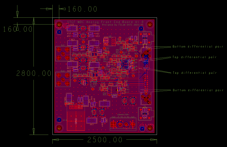
The completed PCB designed in Allegro PCB Editor is shown above. The figure shows only the signal layers, with the top layer in red and the bottom layer in blue. Both signal layers are covered with grounded copper to improve circuit shielding. The size of the rectangular PCB is 2500mil * 2800mil (about 63.5mm * 71.1mm).
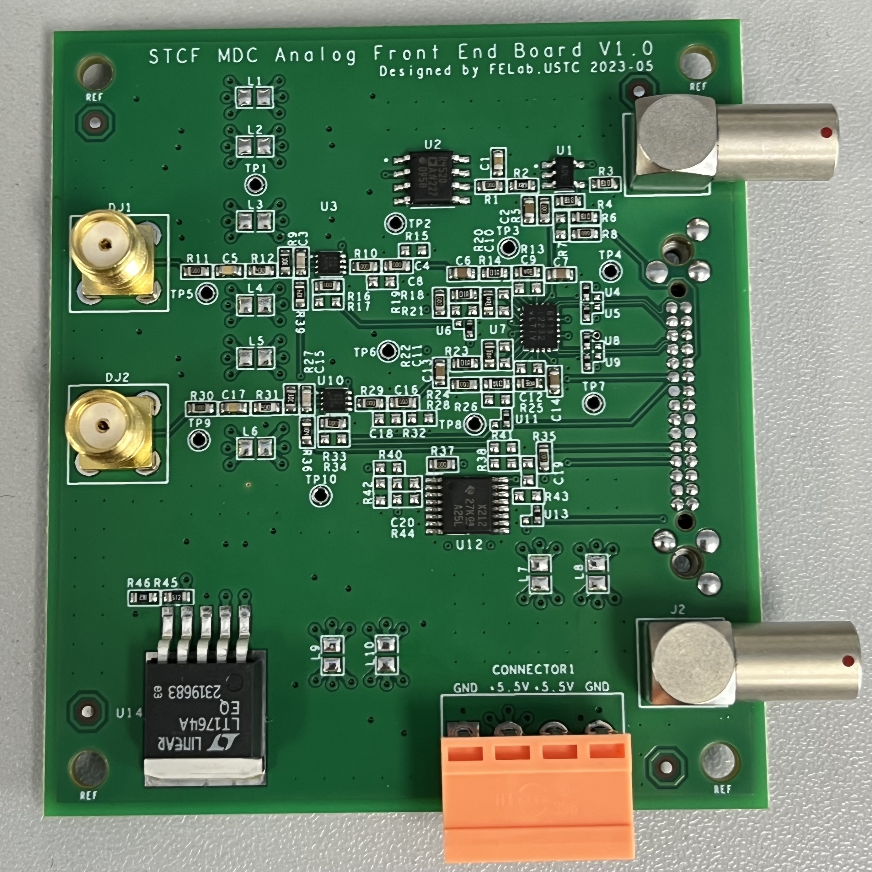
Above is a picture of the real PCB.
Conclusion
In this work, we have designed the schematic and PCB for the STCF MDC detector readout electronics analog daughter board, and have completed PCB manufacturing, elements soldering and preliminary testing, and are in the process of conducting joint testing with the detector. Based on this work, a more refined design is needed to incorporate the latest requirements of the detector and to carry out joint testing with the back-end digital system.
Comments