Take the production of regular shaped SMD (Surface Mounted Devices) as an example.
Making pads
Check the package parameters in the datasheets;
Open Pad Designer and create a new pad file (.pad);
Set the pad parameters
Parameters: Set “Units” and “Decimal places”. Generally, the maximum precision is 2 when the unit is “mils”, and 4 when the unit is “millimeter”.
Layers: To make surface pads, you need to check the “Single layer mode” and set three layers:
- BEGIN_LAYER;
- SOLDERMASK_TOP (indicating that this part is not painted with green oil when making the board, thus giving the pads a window to ensure that the pads are exposed and are actually allowed to solder the area);
- PASTEMASK_TOP (indicating that this area should be coated with solder when soldering) parameters.
Note that
SMD does not need to fill in the “Thermal Relief” and “Anti Pad”.
Generally, the parameters of “PASTEMASK_TOP” are the same as “BEGIN_LAYER”, and “SOLDERMASK_TOP” is 0.1mm larger than the previous two.
Making packages
Placing pads
Open PCB Editor and select “Package symbol” in “Drawing Type” then create a new package file (.dra);
Modify the size of grids appropriately;
Add the pad file directory: Setup - User Preferences - Catagories - Paths - Library - add the above pad directory to padpath, psmpath, devpath;
Add pad pins: Layout - Pins - Select Connect - Select pads from Padstack.
Drawing packages
The package includes (bolded red is mandatory, italic is highly recommended)
At least one pin (i.e. pads);
Graphic border (i.e. Assembly_Top subclass and Silkscreen_Top subclass of the Package Geometry class), indicating pin 1;
Reference number (i.e. at least one subclass of the Ref Des class, usually using the Silkscreen_Top subclass and sometimes drawing the Assembly_Top subclass in passing), placed near the package;
Installation Area (i.e. Place_Bound_Top subclass in the Package Geometry class).
After saving the file, you will get
a .dra file (drawing file, which can be opened to edit the package);
a .psm file (data file, which cannot be edited directly, but is necessary when importing the netlist in the .brd file).
Note that
Draw the outer frame for assembly on “Assembly_Top”;
Draw the silkscreen pattern on “Silkscreen_Top”;
Draw the area without electrical rules to prevent overlapping of devices on “Place_Bound_Top”;
It is highly recommended to put pads, vias and device package files (.dra and .psm) in the same folder.
Importing
Creating a board
Open PCB Editor, select “Board” in “Drawing Type”, create a new board file (.brd), and set the page size and grid point size;
Draw the outer frame of the PCB: Add - Line, select “Board Geometry” in class, select “Outline” in subclass;
Draw the allowed wiring areas “Route Keepin”: Setup - Areas - Route Keepin. It is recommended that it is 30~40mil from the outer frame;
Draw the area “Package Keepin” where the device is allowed to be placed: Edit - Z-copy - Size: Contract - Offset: 1. Generally, indent the “Package Keepin” by 1mil than the “Route Keepin”;
Place the mounting holes and make them tangent to the frame of the “Package Keepin”.
Setting the structure
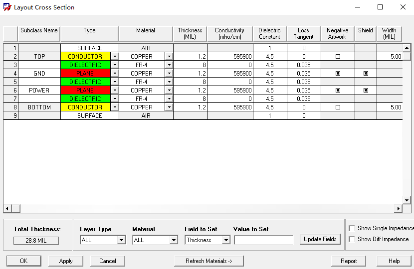
Take a 4-layer board as an example, from top to bottom are
- TOP (top alignment layer);
- GND (ground copper plane);
- POWER (power layer copper plane);
- BOTTOM (bottom alignment layer).
Setup - Cross-section - add the middle layer;
Set the type of each layer (CONDUCTOR for the alignment layer, DIELECTRIC for the media layer, PLANE for the copper plane of power layer and ground layer);
Name each layer;
Set the positive and negative piece (the alignment layer is positive, that is, the drawing is the part to be kept; the copper plane is negative, that is, the drawing is the part to be discarded).

Laying copper in the inner electric layers
With “Route Keepin” drawn, you can use Z-copy to lay copper on the inner layer. At this point, the copper laying of the inner electrical layer is only temporary, just in order to facilitate the subsequent wiring to see if the over-hole is too close. Like the adjustment of the outer frame of the board, the copper plane of the inner layer will be readjusted (i.e., copper re-laying) when the layout wiring is determined.
Select “GND” or “POWER” (respectively for the GND layer and POWER layer copper laying) in “Options”, select “Create dynamic shape” (to prevent short circuit);
Set GND layer “Offset” to 0, POWER layer “Offset” to 40mil (the power layer needs to be indented 40 mil from the ground layer to reduce the outward radiation from the edge of the plate);
Select “Shapes” in “Find”;
Turn off the rest of the internal electrical layer display in “Visibility” (so that when laying copper, you can clearly see whether the copper laying is successful).
You can also directly lay dynamic copper in the GND layer and POWER layer, and then merge and adjust the shape of copper.
Importing the netlist
File - Import - Logic - Design entry CIS (Capture) - Import directory - Import Cadence
If a window pops up, modify it according to the error report and then re-import; no window pops up means the import is successful.
Comments